E Beam Evaporation Thin Film Deposition Pdf

Thermal Evaporation An Overview Sciencedirect Topics
Http Uni Obuda Hu Users Grollerg Electronic Technology 3 Thin 20film 20deposition Pdf

What Is Thin Film Deposition By Thermal Evaporation
Ar Coating Techniques Thin Film Deposition Methods

Electron Beam Source For Electron Beam Deposition Introduction To Jeol Products Jeol Ltd

Physical Vapor Deposition Pvd Methods For Synthesis Of Thin Films A Comparative Study Semantic Scholar

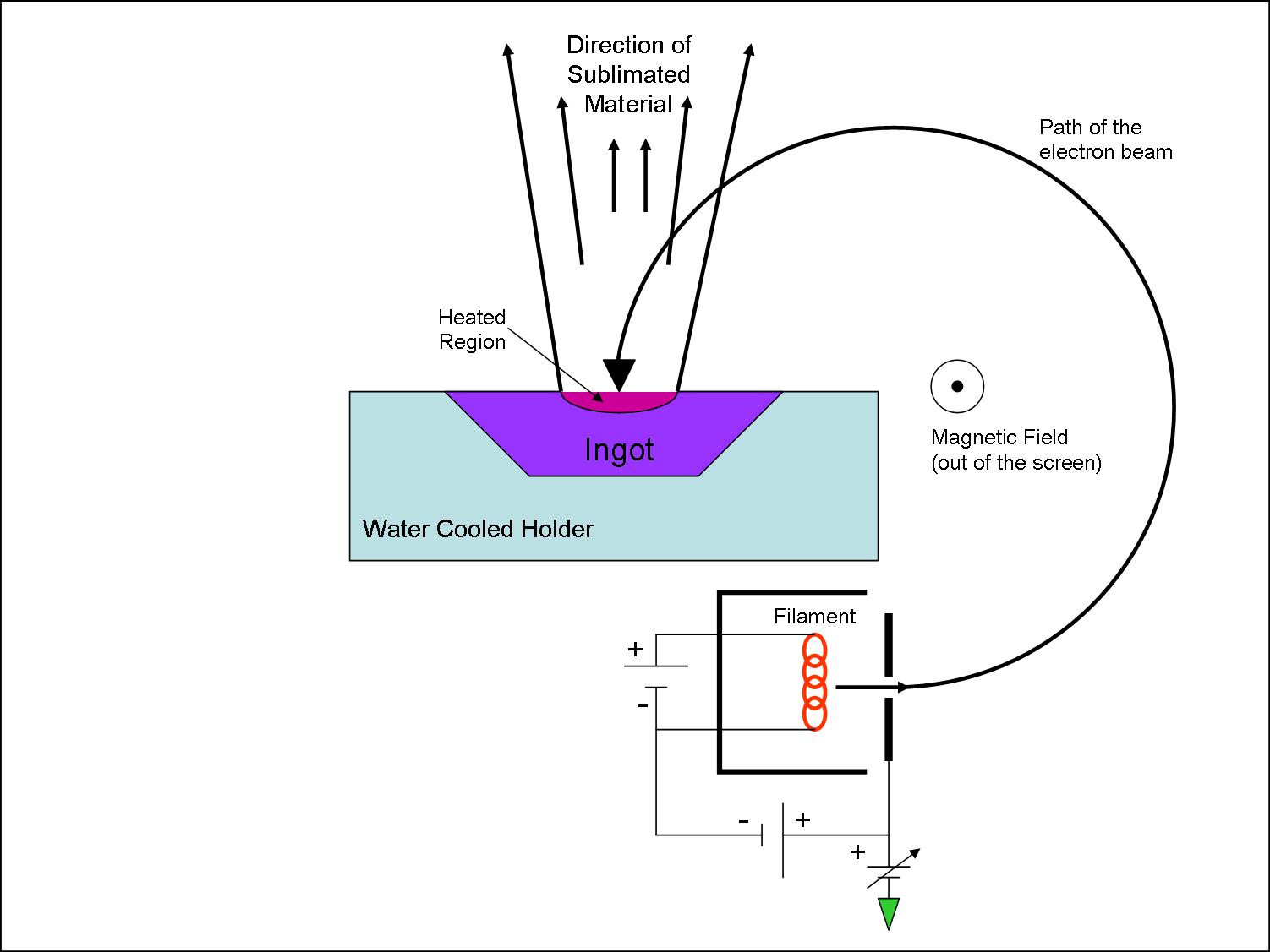
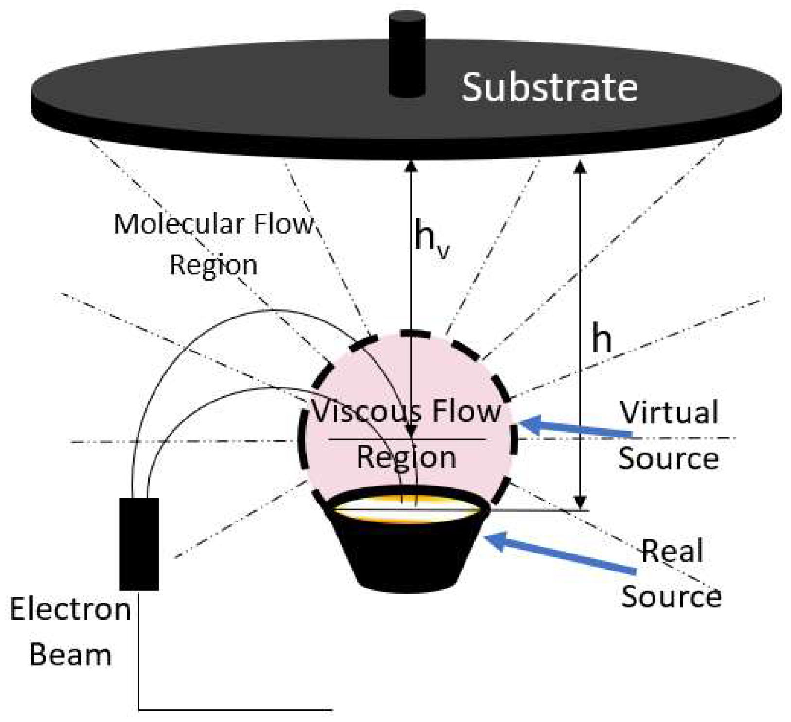
Applied physics 298r 14 e.
E beam evaporation thin film deposition pdf.

Highly Uniform Electrochromic Tungsten Oxide Thin Films Deposited By E Beam Evaporation For Energy Saving Systems Sciencedirect
Pdf Characterization Of Magnesium Fluoride Thin Films Deposited By Direct Electron Beam Evaporation
Https Www Osti Gov Servlets Purl 1145751

Physical Vapor Deposition Ppt Video Online Download

Thermal Evaporation An Overview Sciencedirect Topics
Https Inst Eecs Berkeley Edu Ee143 Fa16 Lectures Lecture06 Thin 20film 20deposition Pdf

Ultra Smooth E Beam Evaporated Amorphous Silicon Thin Films A Viable Alternative For Pecvd Amorphous Silicon Thin Films For Mems Applications Sciencedirect
Pdf Thin Film Deposition Processes

Pdf Wet Etching Of Optical Thin Films

Electron Beam Evaporation Deposition Request Pdf
Coatings Free Full Text Simulation And Optimization Of Film Thickness Uniformity In Physical Vapor Deposition Html

Physical Vapour Deposition An Overview Sciencedirect Topics

Pdf Advance Deposition Techniques For Thin Film And Coating

Vacuum Deposition An Overview Sciencedirect Topics

Pdf Study Of The Optical Properties Of Sio2 And Al2o3 Films Deposited By Electron Beam Technique
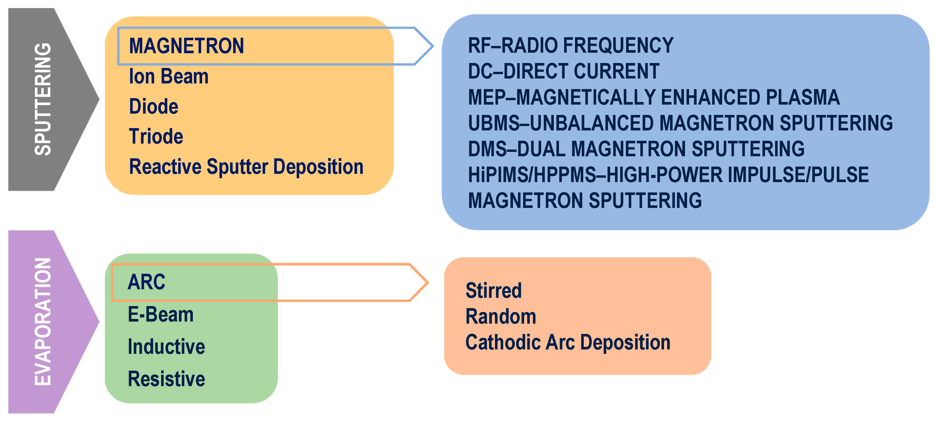
Coatings Free Full Text Sputtering Physical Vapour Deposition Pvd Coatings A Critical Review On Process Improvement And Market Trend Demands Html

Pdf Comparison Of Aluminium Thin Film Deposited On Different Polymer Substrates With Thermal Evaporation For Solar Cell Applications

Explorer Thin Film Deposition Solution Denton Vacuum
Https Encrypted Tbn0 Gstatic Com Images Q Tbn 3aand9gcs1i4bf2tj0ap8dej1oob Kfgi5b4wj Bdloi Oirapr4vxuefg Usqp Cau
Electron Beam Evaporation For Thin Film Deposition

Pdf Materials Science And Engineering Thin Film Preparation Particle Size And Thickness Analysis Experimental Report

Pdf Effect Of Annealing Temperature On Platinum Thin Films Prepared By Electron Beam Evaporation

Pdf Effect Of Deposition Rate On Structure And Surface Morphology Of Thin Evaporated Al Films On Dielectrics And Semiconductors

Alumina Coating Deposition By Electron Beam Evaporation Of Ceramic Using A Forevacuum Plasma Cathode Electron Source Sciencedirect
Source : pinterest.com
